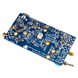
A low-cost DDS module capable of generating waveforms up to about 40MHz. Powered by the ubiquitous AD9850, so it will be easy to find code you will be able to adapt to your own project.
The important pins are broken out to 0.1"-centered headers for simple breadboard usage and project integration. The pinout of the module is detailed below. For more information regarding pin functionality please consult the datasheet linked to above.
| Top Row |
| # |
Name |
Description |
| 1 |
VCC |
Supply Voltage |
| 2 |
D0 |
Parallel Data Interface |
| 3 |
D1 |
Parallel Data Interface |
| 4 |
D2 |
Parallel Data Interface |
| 5 |
D3 |
Parallel Data Interface |
| 6 |
D4 |
Parallel Data Interface |
| 7 |
D5 |
Parallel Data Interface |
| 8 |
D6 |
Parallel Data Interface |
| 9 |
D7 |
Parallel Data Interface |
| 10 |
GND |
Ground Pin |
|
| Bottom Row |
| # |
Name |
Description |
| 1 |
VCC |
Supply Voltage |
| 2 |
W_CLK |
Word Load Clock |
| 3 |
FQ_UD |
Frequency Update |
| 4 |
DATA |
Serial Data Pin |
| 5 |
RESET |
Reset Pin |
| 6 |
GND |
Ground Pin |
| 7 |
QOUT |
Output |
| 8 |
QOUTB |
Comp. Out |
| 9 |
IOUTB |
Comp. Analog Out |
| 10 |
IOUT |
Analog Current Out |
|

